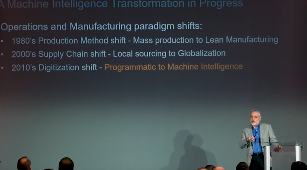
On November 12th, Professor Duane Boning (MIT Electrical Engineering and Computer Science department) announced the new MIT program on Machine Intelligence for Manufacturing and Operations (MIMO) during his presentation to the MIT QUEST for Intelligence audience at the MIT ILP Research and Development Conference. In this session on the Advances in ‘Machine Learning in Manufacturing and Operations’, Prof Boning presented a new AI/ML approach that combines multiple classic ML Methods to address unique challenges in Manufacturing and Operations. Learning about these advances is now available through the new MIT MIMO program which provides Sponsored Research opportunities, MIT MIMO / Quest for Intelligence Symposium Series and Machine Intelligence Survey Participation.
Providing the context, Professor Boning identifies that the thrust of Machine Learning is causing a paradigm shift in Manufacturing and Operations driven by IIoT, the availability of massive amounts of structured data, advances in ML methods and the growth in compute capacity.
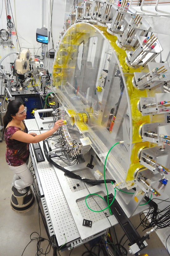
During the presentation he shows machine learning techniques applied to Operations and Manufacturing Use Cases including process control, yield prediction, defect detection, spatial variation reduction and anomaly detection. The presented research accentuates the need to apply the correct Machine Learning methods or combination of methods to targeted Manufacturing and Operations Use Cases. This mapping is especially important due to the unique challenges that arise when applying Machine Intelligence in Operations and Manufacturing; Class imbalance (small data problem), Concept model drift, multivariant time dynamics, domain & underlying physics engineering knowledge and trust.
Professor Boning provided examples of the use of a Machine Learning and Deep Learning in the following areas:
Machine Learning Process Control
Control of the chemical-mechanical polishing of semiconductor wafers. Optimal run-by-run control was achieved by training a Neural Network to select and tune the control parameters of a simple linear feedback control model. Video starts at 7:32.
Yield Prediction and Improvement
Improve chip-stack packaged memory yield. Individual memory chips that tested good in an electrical test are further classified as good or bad using a Random Forest Classifier. The model continually learns to adapt to small changes in manufacturing process (concept drift) through Online/Incremental Learning from new process data. Video starts at 9:33.
Defect Detection and Classification
Defect Detection and Classification: Identify and classify defects on automobile tire treads. Train a Convolutional Neural Network to identify, locate and classify tire defects by using Transfer Learning from a Neural Network pre-trained on ImageNet data. Video starts at 17:20.
Spatial Variation Reduction
Control the sputter deposition process to reduce thickness variation across a semiconductor wafer. Integrate engineering knowledge into a Bayesian Model and use Reinforcement Learning to find the best operating point in a manufacturing process. Video starts at 20:10.
Anomaly Detection in Time Series Data
Identify when a Plasma Etch process starts to make bad semiconductor wafers. Use K-means Clustering on time series data to group similar process cycles together which can then be labeled by experts as good or bad. The labeled data is then used to train a Recurrent Neural Network to alarm when the current process data does not match known good (predicted) data. Video starts at 25:15.